 Strategic Resource Intelligence
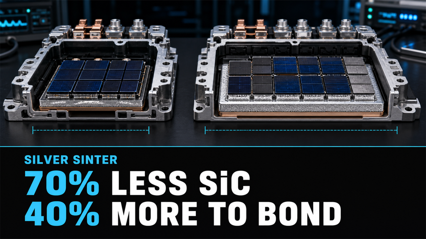
Infineon’s 2026 paper compares three 200-to-300-kilowatt traction-inverter systems in the 470-volt power-net class. The open-loop measurements used a 450-volt DC working voltage, 10-kilohertz switching and 65 °C coolant.
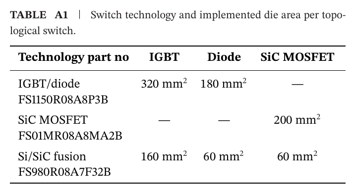
With the same nominal 15-micrometer bondline thickness across all three constructions, the disclosed die geometry can be compared directly. Full SiC used 200 square millimeters per topological switch. Fusion used 60 square millimeters of SiC, then added 160 square millimeters of IGBT and 60 square millimeters of diode. Its total reached 280 square millimeters: 40% more area on silver sinter despite using 70% less SiC.
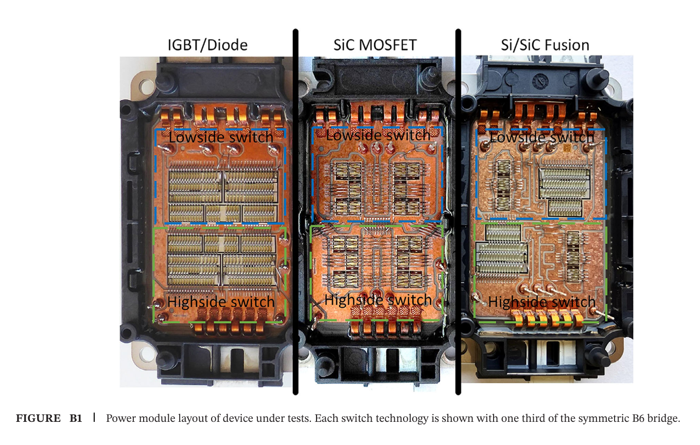
Meanwhile, optimized dead time reduced total inverter losses by up to 5% and improved current sharing within the fusion prototype. Those were control-study gains within that architecture, not a comparison of package economics.
Applying the disclosed 0.015-millimeter bondline across the six topological switches in a three-phase B6 bridge gives the under-die volumes below.
| Architecture | Die Area / Switch | NOMINAL UNDER-DIE SINTER-LAYER VOLUME / B6 | Comparison |
|---|---|---|---|
| Full SiC MOSFET | 200 mm2 | 18.0 mm3 | Full-SiC baseline |
| Si/SiC fusion | 280 mm2 | 25.2 mm3 | 40% above full SiC |
| IGBT/diode | 500 mm2 | 45.0 mm3 | Largest attached footprint |
These are under-die geometry volumes, not paste consumption. A sintered layer is porous, and overprint, organics, process loss, scrap and recovery all change how much paste the factory buys. Infineon published neither paste use nor annual module volume, so no market-demand estimate follows from the table.
What happens on a line depends on more than bonded area. Die count and layout affect handling and inspection. Tooling, applied force and batch loading determine whether a construction still fits the qualified process window. That is where the public paper stops.
An SiC cost comparison starts with the smaller 60-square-millimeter number. For the plant, 280 square millimeters of die still need to be attached. Whether the extra 80 square millimeters disappears inside existing headroom or surfaces in yield, cycle time or inspection requires the manufacturer's own data.
Silver Paste Is Not the Qualified Unit
AQG 324 treats a change in die-attach material or interconnection method as a technology change for an already qualified automotive power module. Released in 2025, the guideline also calls for recording voids, delamination and cracks in the interconnection layer, with scanning acoustic microscopy recommended.
A commercial paste shows why the material name is not enough. Indium Corporation's 2025 InFORCE MF sheet lists 91% silver by weight. For a 5-by-5-millimeter SiC die, its example process uses 12 megapascals at 250 C for three minutes. Printed stencil thickness is roughly twice the final bondline target because the formulation loses about half its thickness during processing, and a different surface can require more pressure or time.
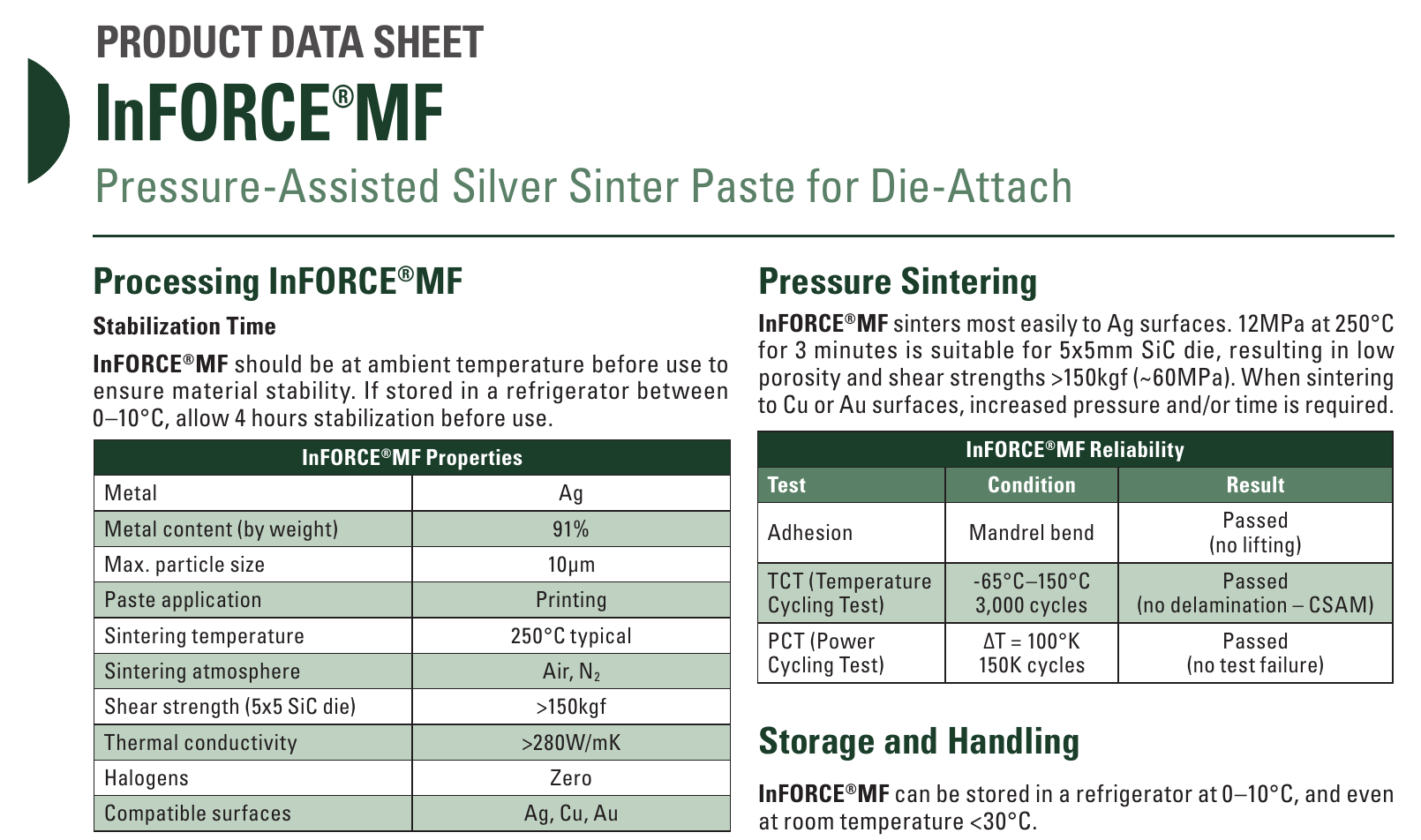
Under AQG 324, the qualified object is the module-level assembly, not a paste in isolation. The guideline does not separately qualify the manufacturing process, but changing die-attach material or interconnection technology requires new qualification evidence for an already qualified module. In practice, material, surface finish, die construction and process settings determine the evidence needed to validate the resulting assembly.
Onsemi's 2025 E1B technical note shows how much the complete construction matters. It describes two silver-sinter interfaces in a stacked-cascode module: one between a silicon MOSFET and a SiC JFET, and another between the JFET and the direct-bonded-copper substrate. At a junction-temperature swing of 100 degrees C, onsemi reports more than twice as many power cycles as an unnamed SiC MOSFET module in the same package.
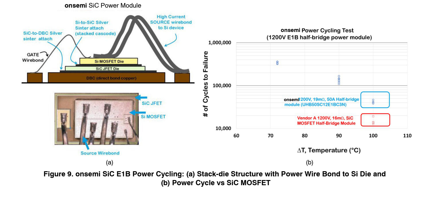
Onsemi's result belongs to the complete construction because the semiconductor architecture also changed and the company attributes part of the mechanical benefit to placing the wire bond on less-rigid silicon. Public evidence cannot isolate either silver layer's contribution, much less transfer it to Infineon's fusion module.
 SilverWars
Put the Factory Answer Into the Architecture Review
Before the design is locked, the executive who owns the module P&L needs an answer from the intended silver-sinter line: can it build the forecast product mix at the required yield and schedule without new capital or a customer qualification delay?
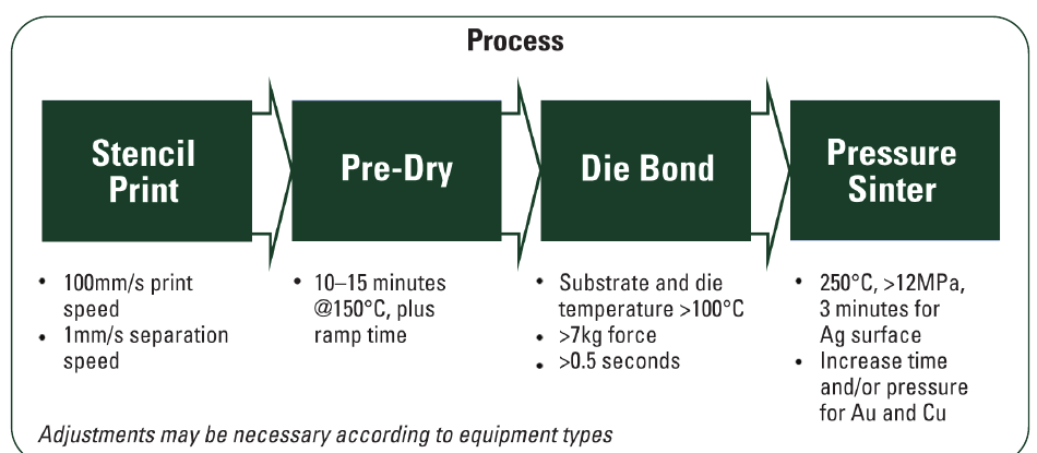
Process engineering can begin with released equipment limits, actual yield data and qualified materials, surfaces and settings. A model is useful for internal screening when the proposed construction stays within those bounds. If it does not, run the construction on the intended line. Quality still has to confirm what evidence the customer requires.
The comparison is economic only when it uses paste per good module and actual yield, not nominal bonded area. It also needs to show what happens to cycle time and utilization at forecast mix, and whether tooling, force limits or customer requalification add cost or time. Put that answer beside the SiC savings case.
The 40% figure earns this comparison, not a presumption that fusion needs more equipment. A prepared line may absorb the larger bonded area with no extra die-attach investment; another may need capacity, yield recovery or requalification time. The P&L owner needs the line result before approving the architecture, when there is still time to adjust equipment scope or the customer qualification plan without moving the launch date.